amr mohamed


Occupation: : 369
Date of Birth : 1994-09-29
Join Date : 2010-11-12
Age : 30
 |  Subject: CMOS ICs Subject: CMOS ICs  Tue 22 Mar 2011, 8:21 am Tue 22 Mar 2011, 8:21 am | |
| CMOS ICs 
CMOS logic family
Adoption of integrated circuits in this family using transistors Mos annularpolar opposite Complementary Mos
The most important features of this family is
1 - low cost.
2 - low power consumption.
3 - resistant to noise performance.
4 - reluctance of income is very high. "
5 - high fan-out.
6 - are available where the key new elements such as analog, which is not available in other families.
7 - circuits can be fed to the efforts of this family, ranging from 3 volts and
V 15.
Defects
Alsemus CMOS
1 - low speed
2 - twice the output current
3 - high price
4 - need special treatment during handling and use
Types of chains CMOS
1 - the series ** CD40
2 - series ** CD45
3 - series ** CD54C
4 - series ** CD74C
Now you will learn about the structure of some of the logic gates in a familyof CMOS and the
Working principles, and consists of the gates of
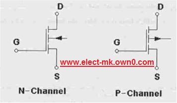
Channel MOSFET transistors and P channel and N, and the symbols of thesetransistors are shown in the following figure

Cyclic codes transistors
P channel Canal N.
Transistor goes with the Channel N
To the state on the application in the event of a positive effort on the gate G, the transistor with a P Channel will move on to the situation in case the application of effort
Or negative (0 zero) at the gate.
The following figure gives the inverter gate in a family of CMOS.

When the input voltage H is in the case of T2 on and off in the case of T1 and the output voltage
Equal to VDS (on) of the transistor T2, and this effort is about "V0.05 which is equivalent to
Low, but when the income is Low, the T1 is in a state on and off in the case of T2 and
Output voltage Vout = VDD and the voltage equivalent to High and the circuit works reflector.
The following figure gives the NOR gate
, and the table shows the positions of transistors and the development of output when all possible cases, logical for the efforts of income NOR gate in the family of CMOS. NOR gate in the family of CMOS.
Work schedule for the NOR gate transistors in the family of CMOS. to the family of CMOS.   | |
|


